
At the TSMC Technology Symposium 2025 on May 15 in Hsinchu, Taiwan, T.S. Chang, VP of Advanced Technology and Mask Engineering at TSMC, announced the company's accelerated fab expansion plans. Previously, TSMC built an average of three fabs annually from 2017 to 2020, which increased to five each year from 2021 to 2024. In 2025, TSMC aims to construct nine new facilities, consisting of eight wafer fabs and one advanced packaging plant.
Fab 20 in Hsinchu and Fab 22 in Kaohsiung, crucial for 2nm technology, began construction in 2022 and are expected to begin production in 2025. Meanwhile, Fab 25 in Taichung is set to begin construction at the end of 2025, targeting advanced technology mass production by 2028.
To address increasing demand from the HPC and AI sectors, TSMC(2330.TW) will expand its advanced packaging capacity. This effort complements current operations and future initiatives at its Kaohsiung facilities, where the company plans to construct five fabs dedicated to A16 and more advanced process technologies.
TSMC plans to start volume production of its 2nm process in late 2025. The rise in AI applications is expected to lead to a twelvefold increase in AI chip shipments between 2021 and 2025. The expanding size of these chips is also driving an eightfold growth in shipments, fueling ongoing advancements in semiconductor technology.
TSMC plays a crucial role in speeding up the adoption of AI technologies.
TSMC utilizes its E-Fab network to leverage its global manufacturing brand advantage. To maintain consistent quality across all locations, the company has created a global management platform that integrates manufacturing knowledge into IT systems. This system encompasses pipeline configurations, raw material quality, equipment parameters, and advanced statistical process control (SPC), ensuring that its overseas fabs align with the high standards set by its Taiwan-based facilities.
TSMC has created a global platform for expert collaboration, allowing real-time experience sharing to address mass production challenges quickly. Its overseas fabs, particularly in the US and Japan, are achieving stable yields comparable to those at its Taiwan headquarters.
At the forum's opening, Ray Wan, director of Asia-Pacific Business at TSMC, highlighted that despite discussions on the Fourth Industrial Revolution happening a year ago, 2024 has seen significant AI-driven breakthroughs in connectivity and computing. These advances earned Nobel Prizes for contributions to machine learning and protein structure prediction, underscoring human ingenuity and AI's transformative potential.
In the AI wave, TSMC is pivotal, delivering smaller, energy-efficient transistors for SoCs and integrating key elements like advanced logic processes, 3D silicon stacking, specialized technologies, and silicon photonics.
In 2024, TSMC shipped 1.8 million wafers in the Asia-Pacific region, contributing to about 10% of the company's total revenue with over 2,400 products. During the year, over 300 new products began mass production.
MediaTek examines key trends in the AI industry.
Joe Chen, MediaTek's COO and president, highlighted three major AI industry trends. Chief among them is the swift progress in model capabilities, particularly through large language models (LLMs). These models have transitioned from simple conversation generators to intelligent agents capable of reasoning and executing tasks. In the future, AI will advance beyond chat tools to become smart assistants with the ability to understand, analyze, and autonomously perform tasks.
Deploying powerful AI models on smartphones could revolutionize user experiences, from enhancing daily conversations to facilitating real-time decision-making, all through mobile devices. This rapid advancement in AI technology surpasses the limitations predicted by Moore's Law, with model capabilities escalating every 3.3 months.
The second trend is the swift improvement of edge computing capabilities. Future smart devices will increasingly use NPUs for AI alongside traditional CPUs and GPUs. By 2028, it is expected that AI-enabled smartphones will comprise about 50% of smartphones worldwide, becoming the norm.
The third trend highlights the integration of AI agent systems with mobile devices, enabling them to seamlessly interact with various applications and platforms by issuing commands and executing tasks. This advancement necessitates open and standardized system interfaces.
Chen highlighted wireless communication and low-power design as crucial for future AI computing infrastructure. The development of 6G standards, which started in March 2025, prioritizes AI-native services in its standardization efforts. To meet high-speed data transmission and computing requirements, MediaTek(2454.TW) is developing interface technologies that achieve speeds of 224Gbps and higher.
Balancing AI performance with battery power in smartphones is crucial. By 2028, AI computing could use over 10 billion kWh annually, highlighting the urgency for energy-efficient AI chip design.


Stay up to date with the latest in industry offers by subscribing us. Our newsletter is your key to receiving expert tips.
2026 has entered its second half.Looking back at the first half of the year, the global semiconductor industry continued to evolve under the strong momentum of AI demand. The rapid expansion of AI ser
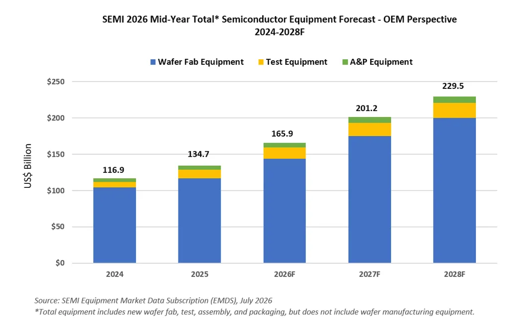
SEMI's latest forecast projects that global semiconductor manufacturing equipment sales will reach a record US$165.9 billion in 2026, representing a 23.2% year-over-year increase. Driven by sustai
According to supply chain sources, memory contract prices are expected to increase significantly over the coming quarters, with gains likely to exceed previous market expectations.Reports indicate tha


